The Center for X-Ray Optics is a multi-disciplined research group within Lawrence Berkeley National Laboratory's (LBNL) Materials Sciences Division (MSD). Notice to users.
News archive
Tailoring Magnetic Skyrmions for Next-Generation Memory
Magnetic skyrmions are nanoscale topological spin structures offering great promise for next-generation memory technologies. However, translating their promise into viable technology requires the ability to modulate skyrmion properties, and their electrical detection under ambient conditions. Partnering with researchers in Singapore we have successfully demonstrated and visualized the control of magnetic properties of skyrmions at room temperature. This was achieved by developing a novel CMOS-compatible thin film material platform enabling the bottom-up control of skyrmion properties. The visualization was achieved by the direct imaging of skyrmions using the CXRO soft x-ray microscope at ALS (BL6.1.2, XM-1). The results demonstrated the ability to modulate the size, density, and stability of skyrmions by varying the thickness of constituent layers - all while using semiconductor industry-compatible fabrication techniques. In conjunction, the world-first electrical detection (Hall effect) of ambient skyrmions was also demonstrated. This breakthrough development provides a stepping stone for realizing stable and highly scalable (10 nm and below) non-volatile memory.
Ref: A. Soumyanarayanan, M. Raju, A. L. Gonzalez Oyarce, Anthony K. C. Tan, Mi-Young Im, A. P. Petrovic, Pin Ho, K. H. Khoo, M. Tran, C. K. Gan, F. Ernult and C. Panagopoulos, Nature Materials, DOI: 10.1038/NMAT4934 (2017).
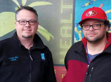
Hero Card Raffle Winner Chanin King Excels at Teamwork
This is an excerpt from an article that originally appeared in “Today At Berkeley Lab”
Safety culture is definitely “a thing” at LBNL’s Center for X-Ray Optics, as evidenced by how research technicians Chanin King and Warren Holcomb identify and resolve safety issues. Chanin won the raffle this quarter for properly tracking and handling unlabeled waste, but both he and Warren have been recognized with a Hero Card on other occasions. For instance, last year Warren received a Hero Card from their supervisor for taking the required steps to resolve a situation that generated static electricity: the equipment was immediately unplugged, a note that described the problem was attached, and their supervisor was notified straightaway so that the issue could be resolved by the appropriate expert.
Chanin lucked out by winning this raffle, but these co-workers feel they hit the jackpot every day just by being on the same team and watching out for each other and their group. When asked about the Hero Card for handling unlabeled waste, Chanin explained the situation but also immediately thought of Warren. That level of teamwork may be present in many work situations but is not always acknowledged so explicitly.
Mi-Young Im takes charge of XM-1

CXRO is very proud to announce Mi-Young Im as the new beamline scientist in charge of our world leading full field soft X-ray microscope (XM-1) at ALS beamline 6.1.2. Mi-Young received her Ph.D. from KAIST in 2006 on the topic of magnetism. In 2007, she joined CXRO and has been a pioneering XM-1 user ever since, with many high profile contributions in nanomagnetism and spintronics. Im's research focuses on understanding fundamental stochastic and asymmetric behaviors in magnetic and spin processes based on direct nanoscale observation of magnetic/spin structures. She currently works on 2D and 3D X-ray microscopy and spectroscopy to tackle numerous scientific and technological problems in nanomagnetic, battery, and catalyst materials. Im plays the central scientific role in CXRO's partnership with DGIST, a world-leading, South Korean national laboratory and research university. This partnership is focused on the development and soft X-ray characterization of emerging materials.
Im's research so far has resulted in 58 papers in internationally peer-reviewed journals and 12 invited talks at major international conferences. Some of her recent high-profile publications include:
- [1] M.-Y. Im et al., Nature Communications 5, 5620 (2014).
- [2] M.-Y. Im et al., Nature Communications 3, 1978 (2012).
LBNL-DGIST collaboration discovers butterfly effect to trigger stochastic behavior in magnetic vortices
Researchers from the LBNL-DGIST Joint Institute of Microscopy have used the unique properties of magnetic soft x-ray microscopy to obtain a deeper fundamental understanding of nanoscale spin behavior, paving a way for potential device applications with unconventional spin textures. However, with current length scales in devices approaching fundamental limits, stochastic, i.e. intrinsically random processes, which so far have been associated mostly with thermal fluctuations, pose severe obstacles. Using the CXRO XM-1 soft-x-ray microscope at ALS Beamline 6.1.2 to study large arrays of asymmetrically shaped magnetic disks, it was found that the ultrafast dynamics controlling the vortex formation exhibits a characteristic chaotic behavior known as a butterfly effect, where minute changes can significantly determine the final outcome of a process. A fully deterministic behavior can be obtained by adjusting the disk distances.
Ref: M.-Y.Im, K.-S. Lee, A.Vogel, J.-I. Hong, G. Meier, P. Fischer, Stochastic formation of magnetic vortex structures in asymmetric disks triggered by chaotic dynamics, Nature Communication 5 5620 (2014)
Peter Fischer Elected APS Fellow

Peter Fischer has been elected as a Fellow of the American Physical Society (APS) Fellow for "contributions to imaging spin structures and their dynamics with high resolution magnetic soft x-ray microscopy.” Fischer is a Staff Scientist at the Center for X-ray Optics, and an Adjunct Professor in Physics at UC Santa Cruz. This is one of the highest honors from APS, and very prestigious. Other APS fellows have been announced for 2014, and Berkeley Lab is well represented.
CXRO launches a website dedicated to Fresnel zone plate theory, design, tolerancing, fabrication, and applications.
CXRO's new website, zoneplate.lbl.gov, provides a full spectrum of information related to the theory, design, tolerancing, and fabrication of Fresnel zone plates. It is separated in to five main areas:
- Zone plate theory: Fresnel zone plate theory and equations. Learn about zone locations, resolution, bandwidth restrictions, and field of view.
- Zone plate design: An easy-to-use zone plate generator / calculator that creates zone plate GDS files to match the wavelength, imaging conjugates, and constraints that the user provides.
- Zone plate tolerancing: Learn how fabrication tolerances affect system performance and how to spec zone plates to optimize performance and minimize fabrication complexity.
- Zone plate fabrication: Learn about fabrication techniques, materials, limitations, and how they impact zone plate performance.
- Zone plate applications: Learn how zone plates enable and impact science and industry around the world.
LBNL-DGIST Joint Institute for Microscopy
CXRO partners with Daegu Gyeongbuk Institute of Science and Technology (DGIST) to form the LBNL-DGIST Joint Institute for Microscopy. The joint institute will harness the power of soft-x-ray transmission microscopy in the characterization and development of emerging and hybrid materials offering multiple functionalities in the realm of energy science, electronics, and biological applications. This partnership will synergistically combine DGIST's strengths in hybrid materials synthesis with CXRO's strengths in nanoscale materials characterization.

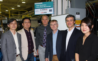
Jung-Il Hong (DGIST), Yong Seung Kwon (DGIST), Steve Kevan (ALS), Peter Fischer (CXRO), Patrick Naulleau (CXRO), Mi-Young Im (CXRO and DGIST)
CXRO helps develop the world's first scanning EUV mask imaging microscope
CXRO has partnered with Samsung to develop the world's first scanning EUV mask imaging microscope. The instrument, integrated by Samsung, uses a commercial high-harmonic generation light source and is now operational in an industrial setting. CXRO's role included system specification as well as design and implementation of the system's diffraction limited optics and detector module. The optics module includes several key new developments: a single harmonic selecting multilayer turning mirror, elliptical zoneplate for off axis operation, a micro-fabricated integrated order sorting aperture, and low-noise detector / electronics hardware for single laser pulse detection per scan point. CXRO also developed controls and image processing algorithms to enable an image reconstruction accuracy in the single digit nm regime.
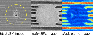
Left: scanning electron microscope (SEM) image of an EUV mask with a defect. Middle: SEM image of printed EUV wafer in the region of the mask defect. Right: actinic image of the mask image taken with the new microscope shows the phase defect printability on the wafer is reproduced successfully in the actinic image.
3D imaging of Ni nanowires
High resolution tomographic capabilities were added to the full-field soft X-ray microscope XM-1. This tool allows to address important topics in the emerging mesoscale sciences. Specific focus of our research targets materials science, environment and energy research. A full 360 angular scans can be obtained within a few minutes of exposure times at 25nm spatial resolution covering a field of view of about 10um.
The first results show a tomographic reconstruction of Ni nanowires (100-150nm diameter), which are explored as a new concept for information storage. The sample was provided by Daniel Rueffer (EPFL Switzerland) and the tomographic reconstruction was done in collaboration with Dula Parkinson (ALS).
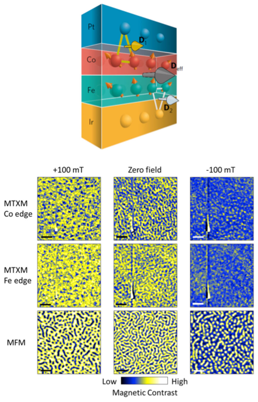
Not all vortex states are created equal
A team of researchers, headed by Peter Fischer and Mi-Young Im of MSD’s Center for X-Ray Optics, in collaboration with colleagues in Japan, have discovered that magnetic-vortex formation in ferromagnetic nanodisks is asymmetric, contrary to common assumption. Their results are relevant to implementing nanodisks in data storage devices as the asymmetry could lead to failure during initialization.
When ferromagnetic materials are formed into nanodisks, the electron spins curl into vortices with needle-like cores. A given vortex state is defined by chirality, clockwise or anticlockwise, and core polarization, up or down: a total of four possible configurations, which were previously assumed to be equally probable.
Employing the unique X-ray beams at Berkeley Lab’s Advanced Light Source, the researchers simultaneously imaged the polarity and chirality of arrays of permalloy nanodisks as they initialized the vortex states. By collecting statistics from more than 1500 measurements, they determined that the generation probability for a given state is not symmetric and that some states are 1–2% more likely than others.
The researchers attribute the asymmetry to a combination of spin–orbit coupling at the disk surface and extrinsic factors like surface roughness.
For more information check out the article "New Phenomenon in Nanodisk Magnetic Vortices".
Partnership for progress in electronics strengthened by new lab-industry investment
Leading semiconductor and emerging-technology firms have recently renewed their long collaboration with the U.S. Department of Energy’s Lawrence Berkeley National Laboratory (Berkeley Lab) to build facilities and instruments for advanced extreme-ultraviolet lithography (EUVL), including microlithography test tools too costly for individual manufacturers.
Since the early 2000s, Berkeley Lab’s Center for X‑Ray Optics (CXRO) has worked with semiconductor companies to develop the infrastructure needed for world-leading research and development in the field of EUVL, contributing basic research and development essential to the health of the U.S. industry as a whole before individual firms enter competition.
“The MET5 will be a unique instrument with double the effective resolution of the best tools now in commercial use,” says CXRO’s director, Patrick Naulleau, a staff scientist in the Lab’s Materials Sciences Division. “MET5 and the new wafer-processing facility at ALS Beamline 12 will allow us to develop and test photosensitive materials capable of transferring patterns on the nanoscale, the future domain of semiconductor lithography technology.”
For more information check out the article "Partnership for Progress in Electronics Strengthened by New Lab-Industry Investment".
Industry funds development of new world-leading full field EUV microscope at CXRO
The Center for X-Ray Optics (CXRO/MSD) at Lawrence Berkeley National Laboratory, in partnership with a consortium of leading semiconductor industry companies, is poised to create the world’s most advanced extreme ultraviolet (EUV) microscope.
This revolutionary imaging tool will be dedicated to photolithography research: photolithography is the central process in the creation of computer chips. The new microscope will replace ageing infrastructure on ALS Beamline 11.3.2 and give the semiconductor industry a nano-scale view into chip making processes in the 16,- 11-, and 8-nm device sizes, for the next decade and beyond of computer memory and microprocessor development.
Years ahead of commercialization, research consortia formed from leading semiconductor companies cooperatively fund the development of chip-making technology. This 1.5-year, $4.1M project will take place in parallel with ongoing operations of the existing EUV microscope, ultimately replacing it and beginning full operations in 2013. The new microscope will reproduce the properties of current and future lithography production and development tools, giving researchers the most advanced look at what’s to come.
For more information check out the article "Sematech Funds Actinic Microscope for EUV Masks".
Paving the way to 16-nm nanoelectronics
In collaboration with Inpria Corporation, the SEMATECH Berkeley Microfield Exposure Tool (BMET) has demonstrated high-quality printing of 16-nm lines and spaces, representing the highest resolution ever achieved from a single-exposure projection optical lithography tool.
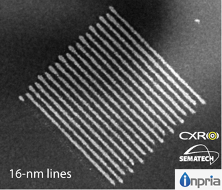
The SEMATECH BMET, built and operated by the Center for X-ray Optics, is used by a worldwide community to study and develop resist materials to meet the future needs of the nanoelectronics industry. The BMET is one of several research tools used to develop and pioneer the supporting infrastructure for EUV lithography, the leading candidate for high-volume manufacturing of nanoelectronic devices with feature sizes below 22-nm. The SEMATECH BMET is unique because its source of EUV light is a coherent synchrotron beamline (12.0.1.3 at the ALS). This source, combined with the spatial filtering property of its central obscuration, enable the SEMATECH BMET to support an imaging resolution of 12-nm. For more information check out the ALS highlight article "Paving the way to nanoelectronics 16-nm and smaller."
Investigating extreme ultraviolet lithography mask defects.
For the first time, using a full-field EUV mask (a mask that contains a real CPU pattern), a group of researchers from Berkeley Lab’s Center for X-Ray Optics (CXRO) has cross-compared the appearance of different types of mask defects recorded in several state-of-the-art tools: the AIT, a scanning electron microscope (SEM), and a commercial deep ultraviolet (DUV) mask inspection tool.
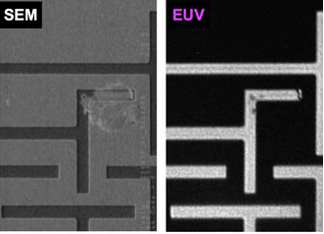
Researchers found that some defects appear to be transparent or thin when inspected with DUV or SEM, but can be completely opaque to EUV light. Conversely, others that appear to be severe defects can be largely transparent to EUV. Phase defects in particular are often subtle and hard to detect with non-EUV techniques, but they can produce a strong intensity-change signature when imaged with the AIT.
Sensitivity differences among the various inspection techniques are caused by the strong wavelength dependence of the defects’ optical properties, enhanced by the physics of multilayer reflective coatings. Currently, the only accurate way to predict the effects of a given defect is to inspect it with the same wavelength used in the lithography process (at-wavelength inspection). Based on the results from the AIT, the semiconductor industry has realized this important point and has recently begun significant investment in EUV mask imaging tools in preparation for high-volume manufacturing.More information on AIT research can be found at http://ait.lbl.gov.
World's first demonstration of 10-nm lens-based full-field imaging.
Using a double-exposure overlay technique, CXRO's Nanowriter team produced the world's highest resolution Fresnel zone plate lens, enabling 10-nm imaging resolution on CXRO's XM-1 microscope.
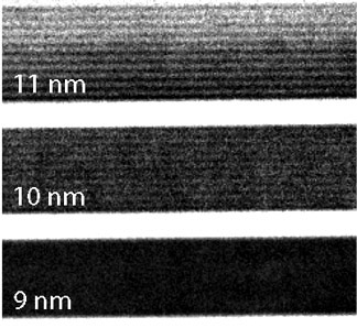
Soft x-ray image of a Mo/Si multilayer test object, demonstrating 10-nm resolution.