The Center for X-Ray Optics is a multi-disciplined research group within Lawrence Berkeley National Laboratory's (LBNL) Materials Sciences Division (MSD). Notice to users.
The world's highest performance microscope for imaging EUV lithography masks.
SHARP High-NA Actinic Reticle Project (SHARP)
In photolithography, a single defect ruins the chip. Our daily work with SHARP answers the semiconductor industry’s most pressing mask R&D questions. We study the unique EUV response to defects, mask architectures, and defect repair strategies.
About SHARP
In photolithography, masks carry the circuit pattern that becomes printed on a wafer (chip) one layer at a time. For EUV lithography specifically, masks are made from ultra-smooth 6-inch glass plates coated with an EUV-reflective multilayer coating, and a patterned absorbing layer on top. The behavior of the entire system, from the glass, to the coating, to the absorber, is highly wavelength specific, so measuring with EUV light is imperative. SHARP is a mask-measuring EUV Fresnel zoneplate microscope that delivers high-resolution images of defects and patterns, years ahead of commercial tools.

Printability studies.
SHARP operates at EUV wavelengths, enabling it to see the true aerial image with high resolution. Researchers use SHARP to study defect printability and to test the effectiveness of defect repair methods.
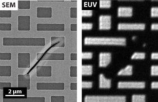
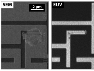
Defects can look very different with different inspection techniques.
Defects that appear severe to visible or ultraviolet light and to electron-beam microscopy can be transparent to EUV light, and vice-versa.

