The Center for X-Ray Optics is a multi-disciplined research group within Lawrence Berkeley National Laboratory's (LBNL) Materials Sciences Division (MSD). Notice to users.
Fresnel zone plates and custom nano-structures enabling novel X-ray instrumentation and nanosicience
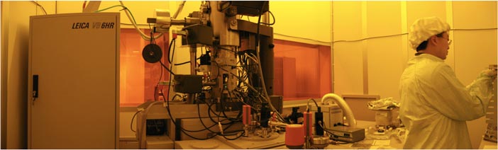
The CXRO Nanowriter Electron-Beam Nanofabrication Lab
"We develop custom nanostructures and unique zone plates for a diverse set of collaborators worldwide. Our experienced team of scientists and engineers is here to push the limits of nanofabrication and diffractive lenses to help scientists realize the unique goals of their research in wide-ranging areas such as nano-diffractive optics, semiconductors, nano-magnetics, and nano-mechanics. When you find yourself in need of nanofabrication expertise for your research or development project, we are here to help."
Weilun Chao,
Nanowriter Team

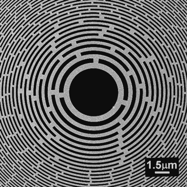
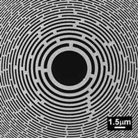
Fresnel zone plate lenses.
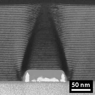
Traditional refractive lenses don't work with x-ray and EUV light because absorption is too high. To bend and focus light at these wavelengths, optical systems must use reflective or diffractive lenses. The image to the left shows a diffractive 'zone plate' lens that was installed at the XM-1 microscope at the Advanced Light Source, enabling 15 nm spatial resolution. CXRO’s Nanowriter is the world’s only electron-beam lithography tool customized to create the curved, continuous shapes that define the zone plate pattern.
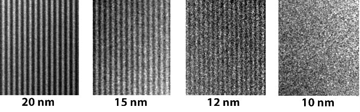
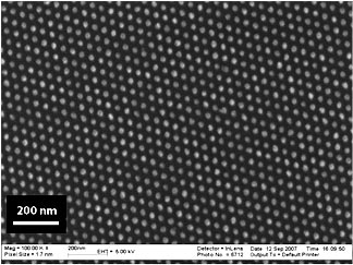
12 nm resolution.
Using a double-exposure overlay technique, CXRO's Nanowriter team produced the world's highest resolution zone plate enabling imaging resolution of 12 nm.
Visit zoneplate.lbl.gov to learn about Fresnel zone plate theory, design, tolerancing, fabrication, and applications.
CXRO's new website, zoneplate.lbl.gov, provides a full spectrum of information related to the theory, design, tolerancing, and fabrication of Fresnel zone plates. It is separated in to five main areas:
- Zone plate theory: Fresnel zone plate theory and equations. Learn about zone locations, resolution, bandwidth restrictions, and field of view.
- Zone plate design: An easy-to-use zone plate generator / calculator that creates zone plate GDS files to match the wavelength, imaging conjugates, and constraints that the user provides.
- Zone plate tolerancing: Learn how fabrication tolerances affect system performance and how to spec zone plates to optimize performance and minimize fabrication complexity.
- Zone plate fabrication: Learn about fabrication techniques, materials, limitations, and how they impact zone plate performance.
- Zone plate applications: Learn how zone plates enable and impact science and industry around the world.
20 years of experience in everything nano.
Block-copolymers
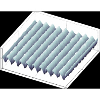
Diffraction gratings (below)
Grayscale masks
Holographic elements
MEMS (below)
Patterned media
Photonic crystals
Programmed defects
Roughness control
Smoothing
System integration
Zone plates (below)
Custom nanostructures. Integration solutions.
A full spectrum of applications. Here are a few examples:
EUV phase-only computer generated holograms.
Diffractive or holographic optical elements can play an important role in lithography systems by providing an efficient mechanism for generating modified illumination. CXRO's scientific team was the first to demonstrate and characterize an EUV binary phase-only computer-generated hologram allowing arbitrary far-field diffraction patterns to be generated. The device shown below achieved an absolute efficiency of 22% into one diffracted order.
SEM image of custom EUV phase-only holographic optical element (HOE) before multilayer deposition
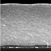
SEM cross-seciton of Mo/Si multilayer coating on 2-nm-tall HOE features.
Far-field +1 order EUV diffraction pattern from the manufactured HOE.
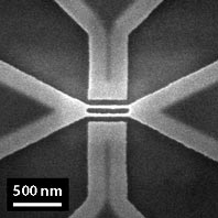
Programmed defects.
Defects buried beneath the reflective multilayer coating can ruin EUV lithography masks. CXRO's Nanowriter is used to create customized, programmed defects for systematic defect detectability and printability studies.
SEM cross section of a programmed buried defect coated with a multilayer.
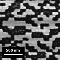
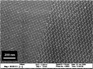
Industry collaboration with Seagate: patterned media.
Templated block-copolymer self-assembly may be a great way to achieve dense patterned media with periods below 20 nm and with long range order over several cm. In collaboration with Seagate, the CXRO Nanowriter has been used to generate self-assembly templates for 0.5 Tb/in2 bit patterned media. Images courtesy of Kim Lee, Seagate.
SEM of 0.5 Tb/in2 pattern generation template
SEM of a servo pattern
The CXRO Nanowriter.
The Nanowriter (below) supports a broad array of scientific instruments and projects worldwide. Its 8-nm beam size, conbined with its 2-nm overlay accuracy enables patterning of dense features down to 10 nm half-pitch.